2010/04/30

Mode 0 / Mode 3 / Mode 4 Tests.

I started to check various ROMs.
Mode 0 seems to be OK.


Then checked mode 3:

This is the screen shot from the emulator.


And here is what I get :


The difference is that I do not have sprites yet, so I can not display the text.
And it also uses HDMA for color rasters, which have dont have yet either.
So for what has been implemented so far, everything is good.

Mode 4 :
I have a glitch, it seems that I read the tile as if it was in mode 16 pixel tiles,
where actually it must access in 8 pixel tile.
Too tired now, I will check that tomorrow. I remember the specs saying that for this mode it MUST be 16 pixels... may be mode 5 ? Too sleepy anyway... Let's save some work for tomorrow anyway :-)

The infamous mode 7.


Ok, I got the mode7 to work today.

There is still some stuff to verify.
The mode7 flip H/W is not working, specification using mosaic and interlace not done yet.
But for most games, it should work as is anyway...
Of course I put the remaining stuff on the TODO list. I do not forget it.

Anyway I posted the pics to show how I tested :-)

2010/04/24

Snes on FPGA Information.

Some of my friends asked me how I could get those screens without having a CPU yet...

Yes, he is right.
What I did is that I wrote a DLL which is plugged into Snes9x.
That DLL tracks every register write to the PPU.

When the "screenshot" feature of Snes9x is called, I also dump the VRAM/CGRAM and all the registers directly into a VHDL program, then I recompile the complete chip and test that particular state.

It is an annoying and lengthy process, as I recompile the chip and resend it to the board,
it takes between 2 to 3 minutes to update a new design, when you also add the time to copy the files from some place to another etc... It is very annoying.

So now I am working on using my serial port and have my DLL do a direct transfer of the VRAM, register states to the chip without recompiling the design.

That is going to be a big plus, it will shorten the debugging time, but also allow me to modify the registers in real time and see if everything is fine.

PS : I forgot to say in my previous post that mosaic is also working nicely.

New screens.


Last time, I did hard code the priority of the BGs,
but now everything is fine.

- The super mario screen now uses MAIN / SUB to display.
- Axelay shadow effect with the space ship at the beginning is OK too.
- Fixed some timing glitches.
- Fixed when PPU is disabled.
- Fixed bug for sprites (palette 0..3 do not participate in Main/Sub color math)


So here are a few screens now.
- Konami logo booted from Axelay
- Village from FF6
- Fortress from FF6.

I think have things to fix of course, but things are getting nicer little by little. :-)

Now it finally start to look like a Snes ;-)


2010/04/18

VHDL Code for the Snes.

I decided to post my code on Google Code repository to allow me to work easily with SVN.

Here is the URL : http://code.google.com/p/fpgasnes/

If anybody is interested to keep in touch with me :
I have a hotmail.com account and you know my nickname :-) so it is :
[my nickname] @ hotmail.com

No MSN please, I am quite busy and do not want to be disturbed at work.

Something to show...


Well, I bet nobody comes on that blog still.
But anyway I am going to publish the results of my work.

I have complete what I think is a good beginning of the Snes PPU chip.
It has all the logic/structure for everything except sprites.

Of course, some inner part are still untested but structure is inside and timing is thought at least.

Now what been proven work on my FPGA board.

- BG 1/2/3/4 memory access for all graphic mode done.
- Of course support for various bitmap format of each mode.
- Support of tile flip 8/16 pixels.
- Support of map of 32/64 tiles mode.


Out of three bugs I was looking for, two were related to SPEC miss.
(Document are not accurate in two places)

My own bug were :
- I had to disable the register writing side of the PPU that went berserk and destroyed the test data.
- I use a modified version of Snes9x with a custom DLL to trap all the call to the registers and dump memory into VHDL tables to be able to take a "screenshot" of the graphics chip state and compile it in my design to verify if the chip does the rendering correctly.
(Big-mega-thanks to ThunderZ for the support, and also future BSnes patching, being too much busy with other stuff)
My DLL for-loop that was dumping the table had A BUG. I lost two weeks because of a LOOP in C++ where like 4000 lines of VHDL CODE WAS CORRECT RIGHT AWAY WITHOUT ANY SIMULATOR !!! Shit... gotta kick my ass sometime.


What remains soon :
- Mode7 need to be finished.
- Mosaic is half-baked.
- Verify and debug window / main-sub variation.

What remains later :
- HiRes
- Interlace (need to check what that means... the chip already actually work at double resolution)
- Sprites

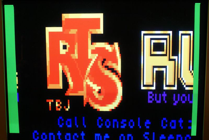
Here's some pix for the curious :


Trying to debug... GARBAGE. Divided the screen in 32 pixel height block and value reflected internal register value.


After finding that I was reading garbage and that my register logic cpu-side was going berserk and I fixed it, I started to have something like that after a few hours of debug.


And after a whole week-end, it gives something like that.
Still my main-sub unit not beeing ready, I hard coded the priority just to display the 3 BGs correctly.

2010/04/04

Snes on FPGA.

I am working since a few weeks (7 weeks) on a Snes on FPGA.

For now I am focusing only on the graphic chip and the chip implementation reaches now around 6k lines of VHDL code and I started the debug a few days ago.

Let's see if I can start to have something consistent to publish within a few feeks from now.
(ie screenshot would be nice)

Cheers.